
Lifetime access • One-time payment • Free updates • No renewal
Full course access: €2495 (excl. VAT)The Electronic Product Development Course
University does not prepare you for real-world hardware design problems
What to do when your design behaves differently than theory predicts
University spends very little time teaching you how to prevent real world hardware problems.
This puts you at a huge disadvantage:
- Signal integrity issues
- EMC problems
- Crosstalk
- Grounding mistakes
- And that's just the start...
The consequences are bigger than most people expect:
- Every design feels like reinventing the wheel
- Months of trial and error
- Multiple unnecessary PCB spins
- Frustration and stress
- And a lot of money burned
In most Western countries, an engineer easily costs €4,000 - €8,000/month to an employer.
So every “learning experience” gets very expensive very quickly.
And the worst part?
Most of these problems are predictable if you know what to look for and have a system to avoid them.
I had to make all those mistakes at great cost as well, until I developed that system.
That’s exactly why I made this course, so you don’t have to go through the same costly learning process I went through over the last 30 years.
Course Contents
The course consists of 2 parts:
PART 1: All the theories and pitfalls you need to be aware of to stop preventable mistakes.
PART 2: Highly detailed design process for a 14-bit arbitrary waveform generator showing exactly how to apply everything you learned in part 1.
PART 1: THEORY AND PITFALLS
PCB parasitics rules of thumb, where do currents flow, ground planes and ground obstructions, unwanted antennas, via impedance, layer assignments, signal crossing, signal bounce between layers, crosstalk theory, problems with loose copper planes, LC filter layout impact, simple rules to prevent grounding and crosstalk problems, exceptions to the rules, real life examples, countless measurements to prove the theory and bad grounding advice you find everywhere and need to ignore. You can watch this module for free.
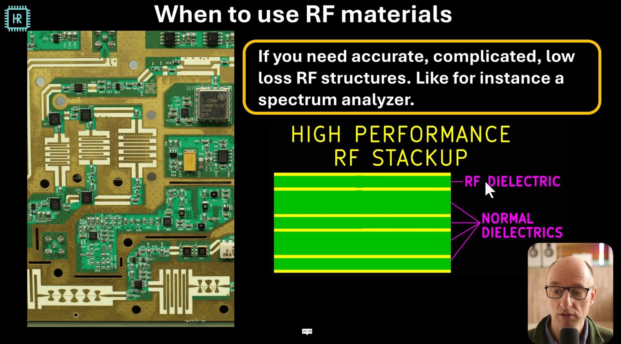
Transmission line basics, why and when do you need them, calculating wavelength, what happens at impedance transitions, reflection calculations, easy reference graphs for return loss, insertion loss, reflection coefficient and VSWR. PCB transmission lines and PCB technology, RF PCB materials, impact of PCB parameters and when to use RF materials. PCB transmission line types: microstrip, co-planar microstrip and stripline and how to get their dimensions, impact of dimensions on parameters, impact of Er tolerances, transmission line crosstalk theory and how to minimize it, near and far end crosstalk, differential transmission lines and dimensions and how to transition from PCB traces to cables.
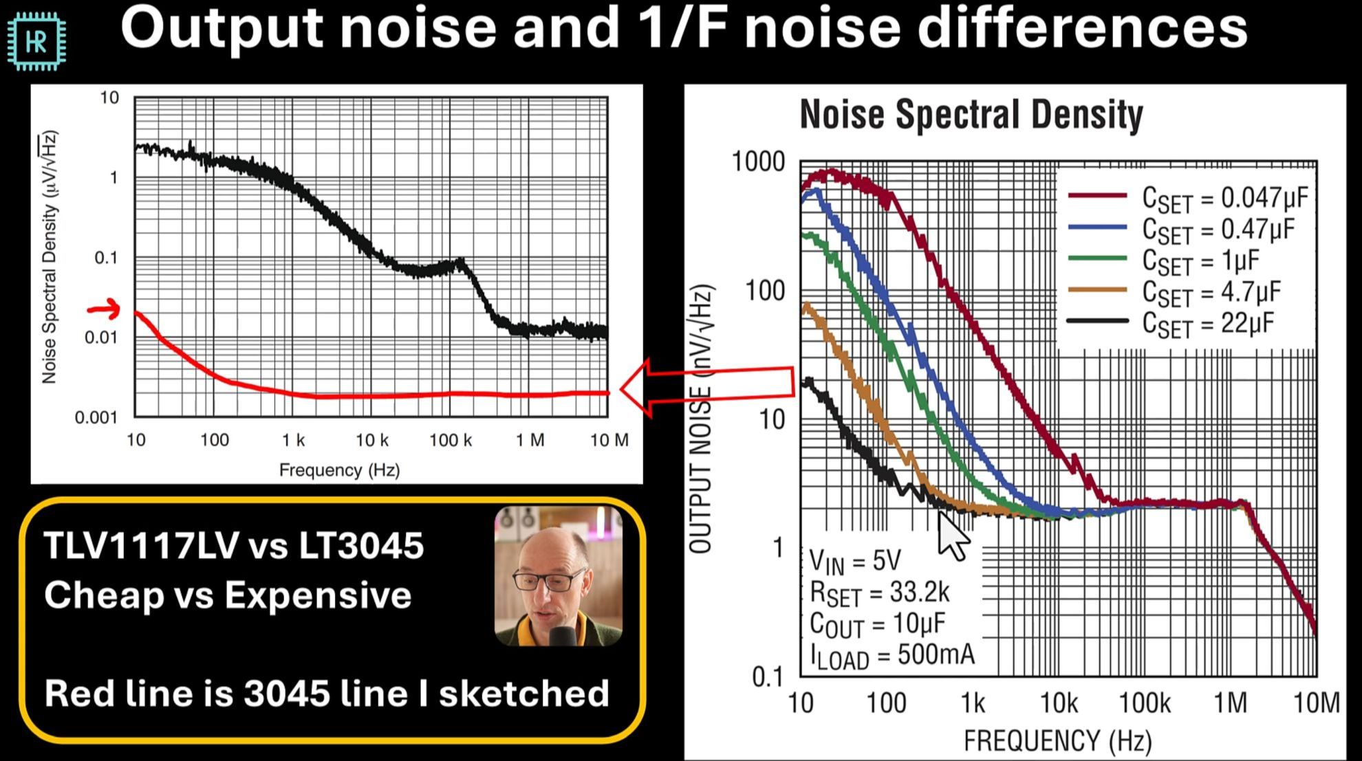
Capacitor limitations: tolerance, bias derating, temp derating, resonance, lifespan, leakage, microphonics, 1/f noise, temperature coefficient and ESR. Capacitor models and how to get them, different capacitor types and their characteristics, class I and class II ceramic capacitors, capacitor overview sheet: all characteristics and pitfalls in one glance.
Inductor types, inductor models, inductor shielding, air gaps and magnetisation curves, inductor limitations: tolerance, derating, losses and resonance frequency. Inductor overview sheet: All inductor characteristics and pitfalls in one glance.
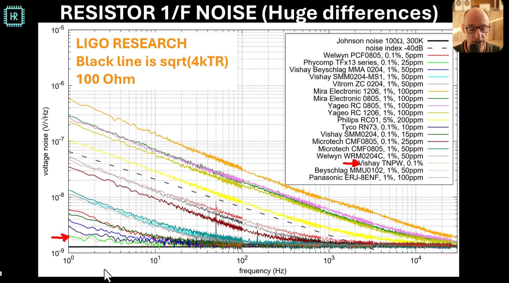
Resistor types: carbon, metal oxide, thick and thin film, wirewound and bulk metal foil. Resistor limitations: Tolerance dissipation, 1/f noise, distortion, temperature coefficient and inductance. Precision resistors, current sense resistors, microwave resistors, resistor overview sheet: all characteristics and pitfalls in one glance.
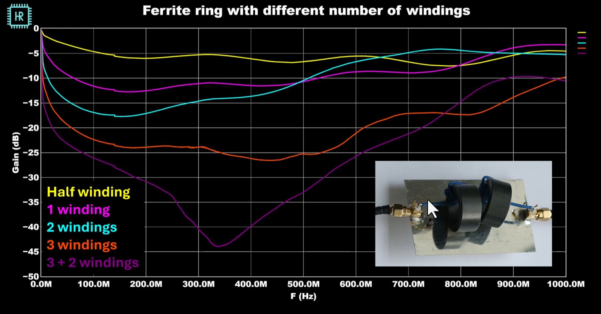
Basic theory on where interference comes from, conducted and radiated interference, CM and DM interference, dealing with radiated emissions, shielding and shielding materials, calculating shielding effectiveness, skin depth, material differences, mesh shielding and mesh size, EMC zoning, dealing with conducted emissions, capacitive filters, inductive filters, CM transformers, ferrite clamps and rings, where to place EMC measures and why, strategies to get signals in and out of shielded systems, types of cables and their effects on EMC, advantages of differential signals, connecting cables to PCBs without issues, understanding the time and frequency domain, what are harmonics, risetime vs interference, problems with fast pulses, understanding how digital signals generate interference and how to minimize it, power supply interference, mains filters and their characteristics, how ESD is generated, ESD testing methods, where do ESD currents go, preventing ESD, circuit protection, transguards, digital busses and ESD and LF ground loops.
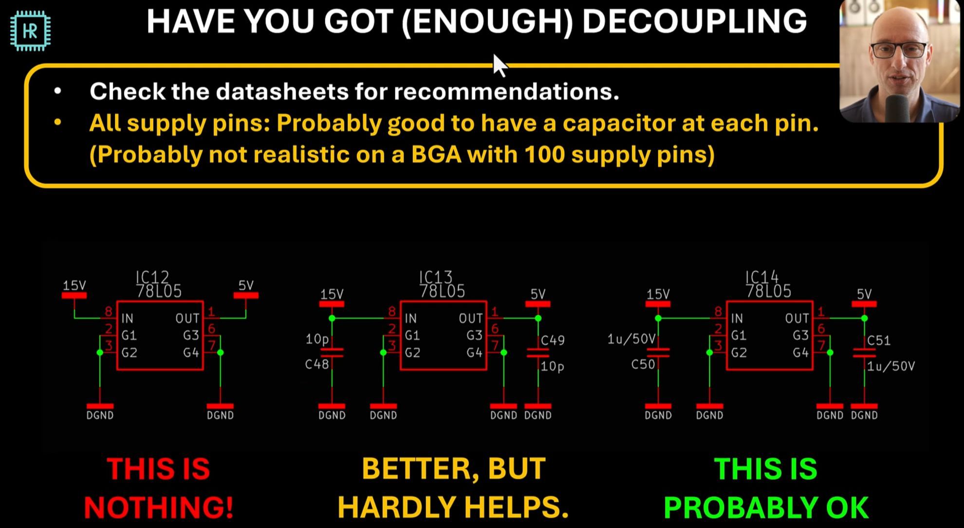
Why supplies can be just as important as grounding, supply design approaches, sensitive circuits, types of regulators, simple models for all regulator types, design procedures for linear and switching supplies, explanation of all supply parameters: tolerances, dissipation, PSRR, dropout voltage, maximum current, ripple and noise, EMI, pricing and tradeoffs. Supply layout attention points, supply filtering methods: trade-offs and pitfalls, combining DCDC and linear regulators, ESR, decoupling strategies, capacitor modelling, pitfalls in decoupling and strategies to solve it, decoupling placement and supply routing. A brief intro to advanced supply design. Measurements to support the theories.
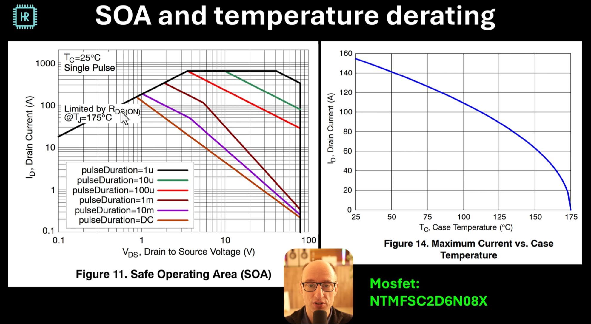
What is reliability, the general approach to increasing it, electrolytic capacitor lifespan and how to maximize it, resistor lifespan, other parts that are prone to failure, the impact of temperature on reliability, thermal calculations, thermal parameters you regularly encounter, regulator dissipation example, heatsinks, passive and active cooling, absolute maximum ratings in datasheets, safe operating area and derating, MTBF curves and failure theory.
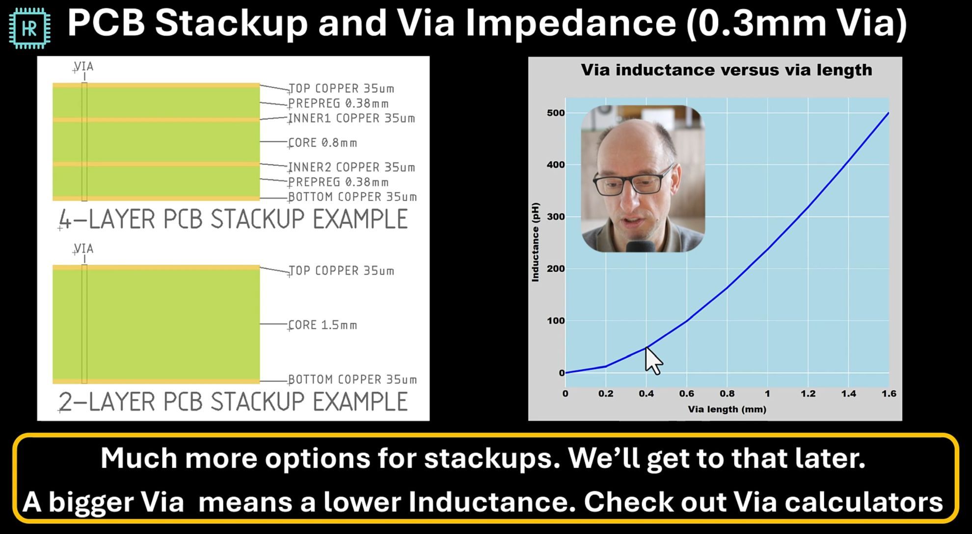
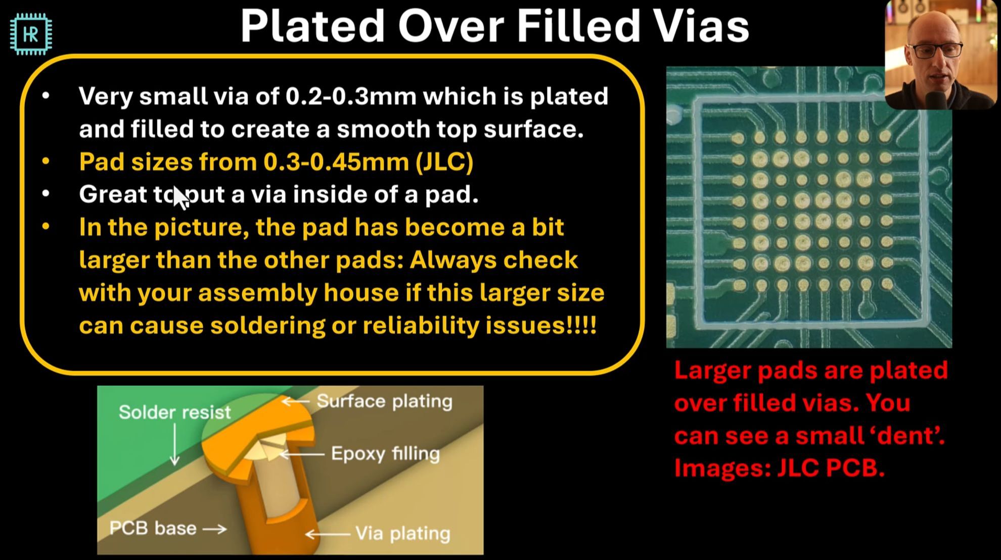
Types of vias and their characteristics: Through hole, microvias, plated over filled vias, blind and buried vias, staggered and stacked vias. Via type price implications, via reliability, via dimensions and rules. PCB stackup options, copper thickness options, detailed layer buildup explanation, RF dielectrics, flexible PCBs, design rules for traces, maximum trace current, trace isolation rules, distance to PCB edges, thermal reliefs, solder masks, surface finishes, cream/paste layers and reflow soldering, copper balance, fiducial marks and courtyards for manufacturability.
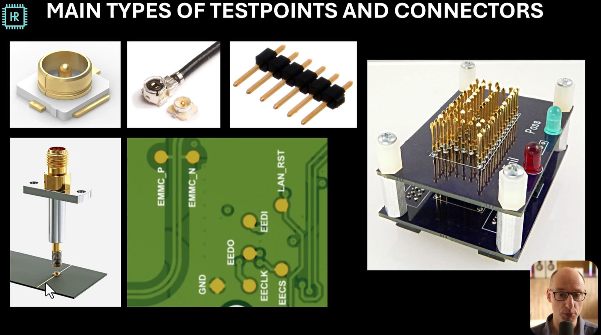
The goal of test and debug options, types of testpoints and connectors, supply voltage and current test options, DC startup tests, RF test options and how to layout them, spare IOs for debugging, options for assembling different types of crucial parts, options to test multiple RF parts and pcb temperature sensors.
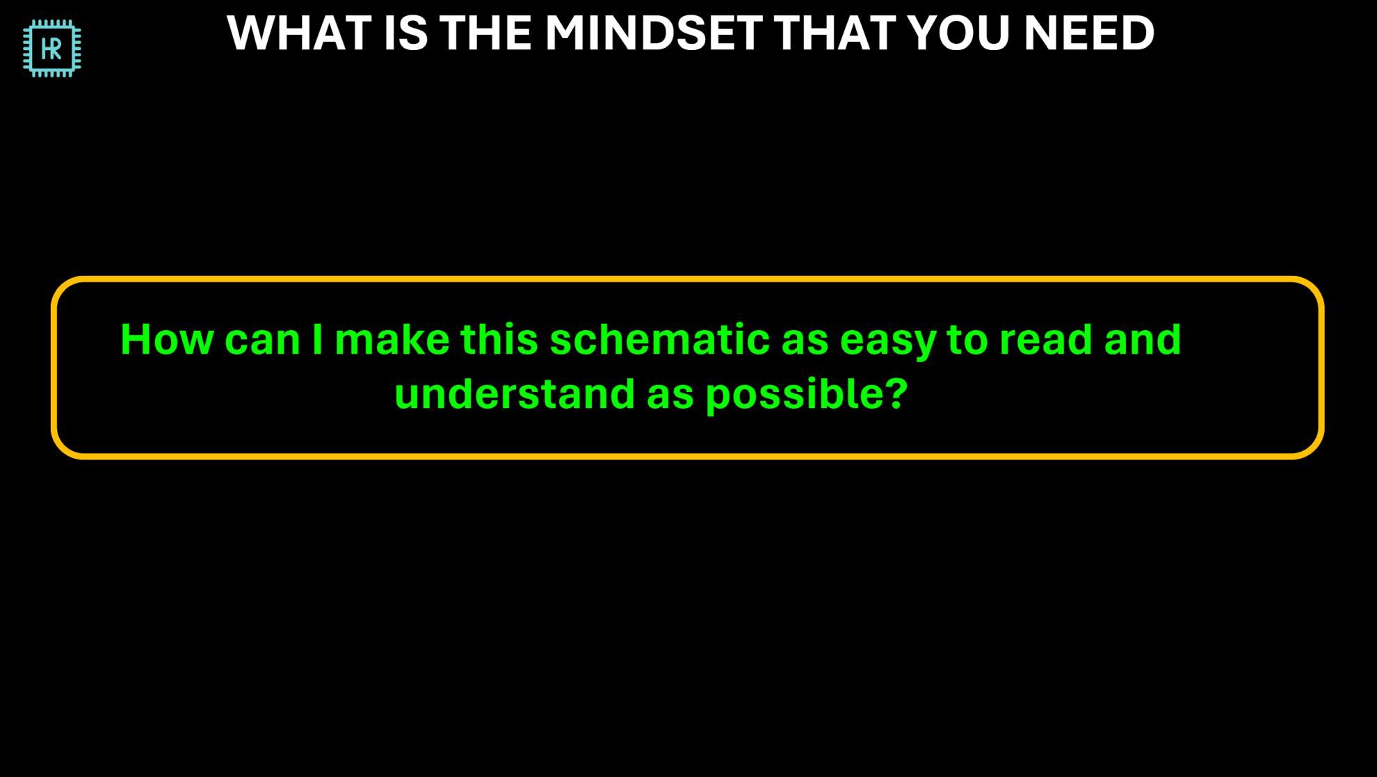
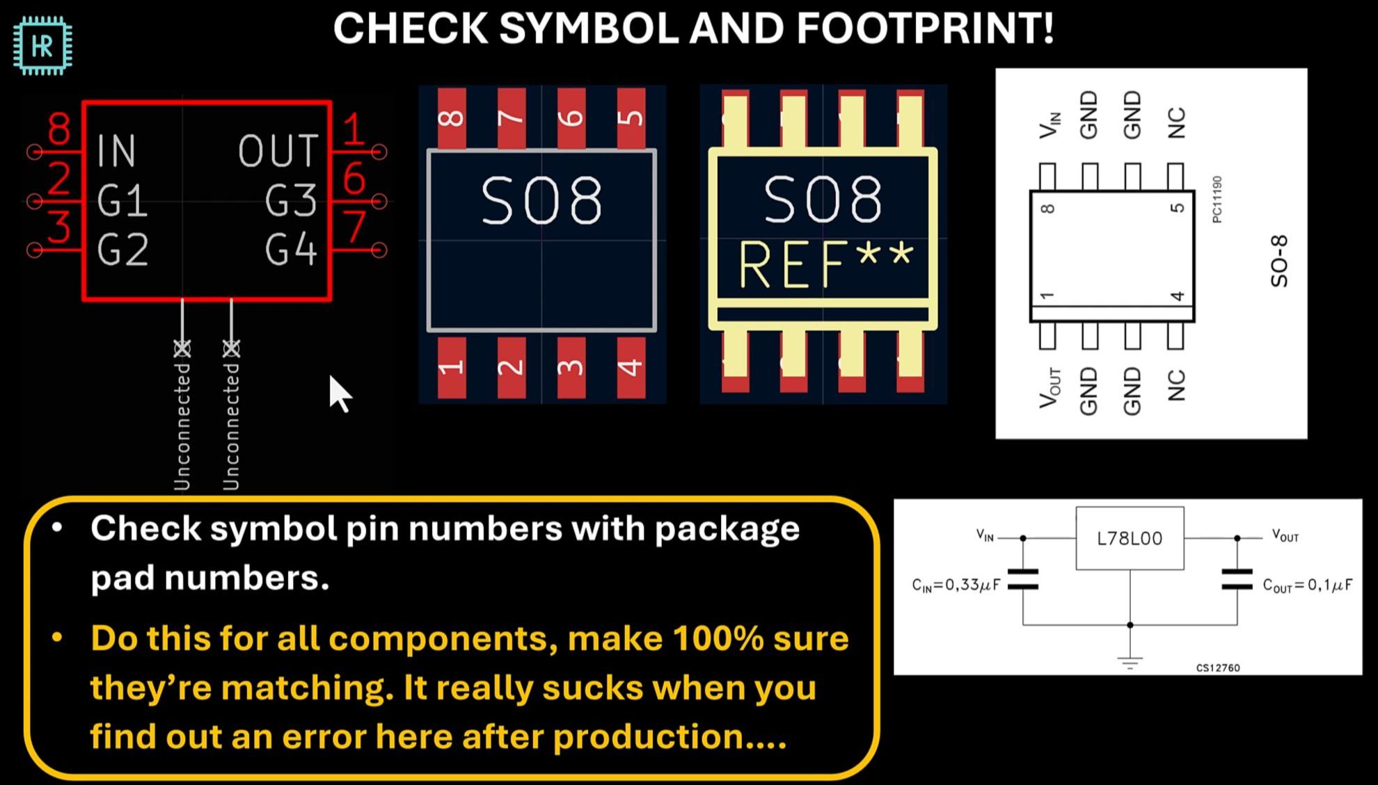
Drawing readable schematics is a highly underestimated but crucial skill to prevent problems. What is the worst possible drawing style, general mindset for drawing schematics, example of a hard to read schematic and how to solve all the problems with it: Block diagrams, making the supply flow easy to follow, grouping functions in a logical way, where to draw decoupling and using the right labels and label names. Creating readable schematic symbols: bad and good examples, general schematic drawing rules, pitfalls when using multiple sheets.
PART 2: PRACTICAL APPLICATION
A 14-Bit mixed-signal arbitrary waveform generator PCB
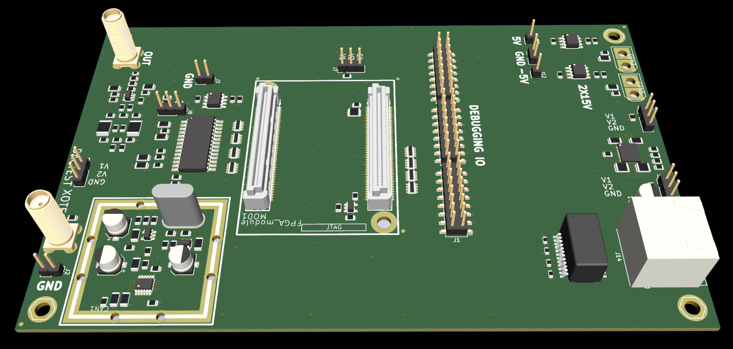
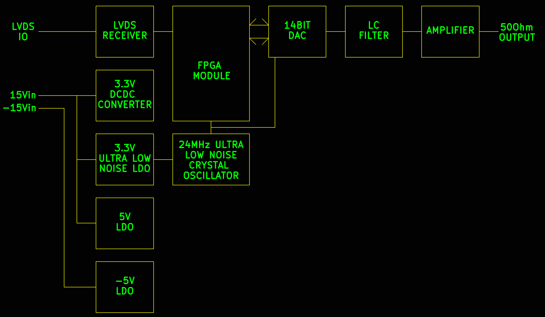
Learn how to convert the block diagram of the waveform generator into a detailed schematic using datasheets and all the knowledge you've learned in part 1 of the course. For each component on the PCB, a conscious choice is made on what to put there.
A detailed example on how to do this is shown after which you can decide to do the rest yourself and compare it to how I would do it, or just watch how I finish the schematic.
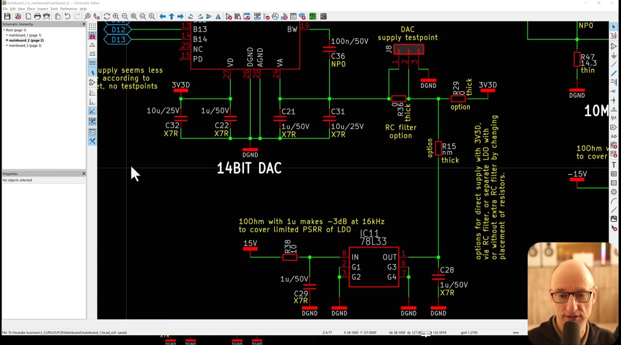
Explanation of a list of checks you can do on a schematic to prevent a number of common pitfalls.
After the explanation, you can use it on the project schematic as there are some errors in there on purpose. You can try to find those or let me show you what they are and how to correct them.
Learn how to do component placment correctly. This is absolutely crucial for achieving good results. A demonstration is given on how to do that after which you can decide to finish the placement yourself and compare it to how I have done it, or just watch how I do it.
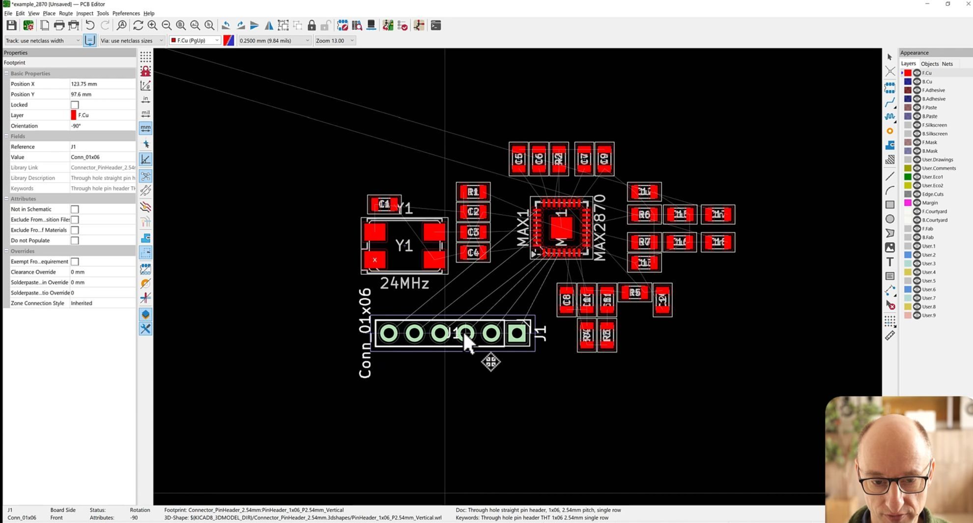
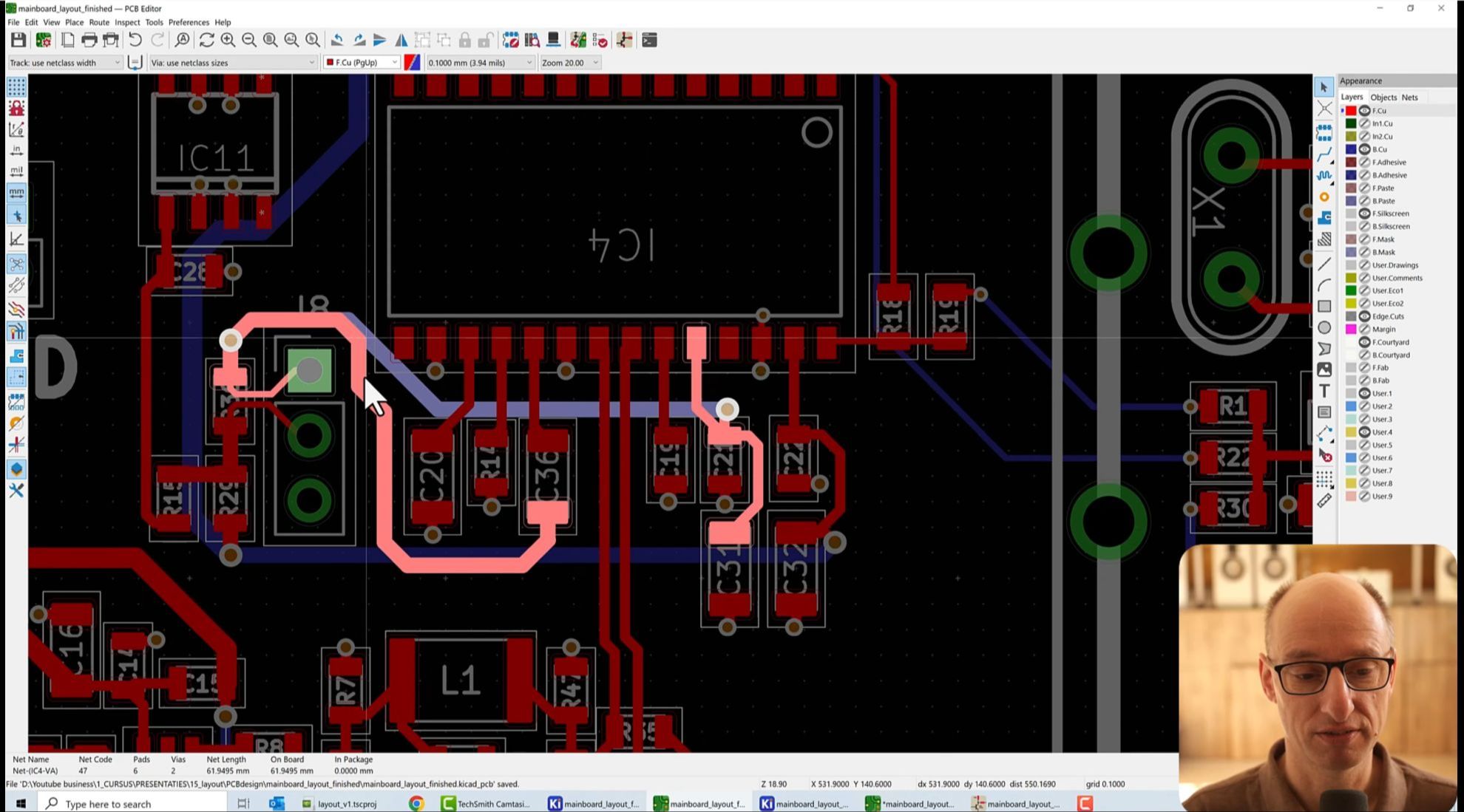
Learn how to layout the generator PCB. Again, I'll show an example of how to do it after which you can decide to do it yourself and compare it to my solution, or to just watch my solution.
Explanation of a list of checks you can do on a PCB and the libraries to prevent common problems.
The correct mindset for preventing problems before they occur and ways to look at designs so you can come up with better solutions. These ways of thinking are absolutely crucial to me.

Nikola Manolov
One of our mature products was struggling to pass recertification, and we couldn't figure out why. Thanks to a tip from Hans's free module and a simple layout tweak, it passes easily now. Invaluable insight for working with regulated products.
Student project: Power Supply EMC
A company making industrial remote sensing rigs had a problem with one of their supplies: it was radiating excessive emissions.
After redesigning the supply using this course, the emissions dropped below the noise floor of the measurement setup in the first bench test.
You can see the results in the spectrum analyzer image below.
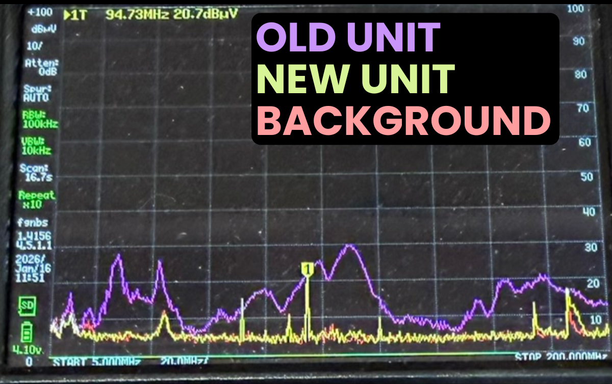
In this rough pre-compliance bench setup, the yellow trace closely follows the red trace across the measured band, indicating that the redesign is effectively at the measurement noise floor, with only minor deviations.
In this one-to-one comparison peak emissions are reduced by up to 25 dB.
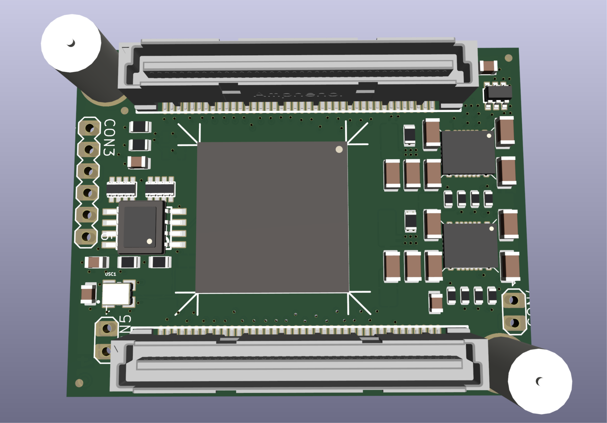
Coming soon: Low EMI FPGA PCB
I'm currently working on this PCB. It's the FPGA module for the Arbitrary waveform generator project in the course. It's also the digital core of my audio DAC.
Most FPGA PCBs are designed around maximum IO and functionality, not low interference.
For my projects, I never need lots of IOs or memory, but I always need very low interference.
So I started designing my own FPGA boards 12 years ago.
When I've designed, built and tested it, I'll add the whole detailed design process to the course as a separate module. This type of design will allow me to demonstrate a number of techniques that are not possible with the main board.
The course has lifetime upgrades so you'll automatically get access to it. There are more projects that I'd love to add.
Program Access & Pricing
€2,495 ex VAT
Lifetime access • One-time payment • Free updates • No renewal
What you get
✅ 10 hours of structured online video lessons
✅ Personal support in private forum
✅ Full KiCad design assignment
✅ Many measurement-based demonstrations
✅ Lifetime access + all updates (like the FPGA PCB)
✅ Certificate upon completion
✅ 14-day money-back guarantee
What you'll learn
✅ How to make a layout that has the least impact on performance (Zero impact is physically impossible)
✅ How to create transmission lines with the best possible performance
✅ How to choose the right passive components to avoid unexpected behavior
✅ How to prevent EMC and ESD issues at the design stage
✅ How to choose the right supply solution for your designs
✅ How to design for long-term reliability
✅ How to design for good thermal performance
✅ How to choose the right PCB technology for your application
✅ How to make your design testable (lab + production)
✅ How to draw schematics to prevent design errors
✅ How to apply all of this in a full, detailed walkthrough of a complex mixed-signal PCB design
I want to say something about the design philosophy of the course material
I once bought a 100-hour course and never used it. The information density was too low to be practical.
I designed this course differently
✅ A maximum amount of knowledge in minimal time
✅ Very practical explanations you can directly use
✅ Explanations are as simple as possible, even for complex subjects
✅ Clearly indexed lessons so you can easily find subjects
This is exactly the same teaching style I use on YouTube and it allows you to revisit any topic in under half an hour when you need it.
I love electronics, and I want this course to be the life-long resource you actually use.
If you have any questions or want to talk to me directly: Just send me an email: [email protected]
Full course access: €2495 (excl. VAT)14-Day Money-Back Guarantee
Watch the first 3 modules within 14 days. If you're not satisfied, you get a full refund.
If you request a refund, I offer an optional short call. Not to keep you in the course but simply to understand what didn’t meet your expectations so I can improve it.
It took me 31 years to develop this system to prevent mistakes that lead to respins or long debugging cycles. In a professional setting, a single PCB respin or debugging cycle often costs more than this entire course.
If you want to see exactly how I teach: Watch the free module first
FAQ
Why is this course €2495?
This course is designed for professional engineers working on real hardware designs.
In many cases, companies purchase this course for their engineers.
In a professional setting, a single PCB respin or a few weeks of debugging often costs more than this entire course and you will encounter multiple of these problems over time.
If you are working on real products, the cost is usually negligible compared to the time and risk it helps avoid.
If you are working purely as a hobby, this course is probably not the right fit.
Why don't you sell separate modules?
Because in real designs, you usually need almost all of them.
If you leave one out, that is often exactly where the problem appears. I have seen this repeatedly over 30 years of design work.
I do not want to sell half solutions.
Am I skilled enough / too skilled for this course?
If you understand basic electronics and can read schematics, you're ready. No RF, EMC, or high-speed experience required.
If you continue designing electronics and PCBs, you will eventually run into these problems so it's better to learn how to avoid them sooner.
Even experienced engineers benefit from the deeper reasoning behind why certain approaches work and how to prevent issues that lead to respins, production delays, and field failures.
Do I have time for this?
The course contains about 10 hours of video lessons. Most engineers finish in 2–4 weeks, often while applying the concepts to their own projects.
You have lifetime access, so you can take it at your own pace: start now, return later, or enroll now and save it for your next design project. Many students revisit modules whenever specific challenges arise.
What if I don't like it?
Watch the first 3 modules within 14 days. If it’s not what you expected, email me and I’ll refund you in full, no conditions. Optional feedback is welcome to help me improve.